- 您现在的位置:买卖IC网 > Sheet目录2008 > MAX1240AEPA+ (Maxim Integrated Products)IC ADC 12BIT SERIAL 8-DIP
__________________General Description
The MAX1240/MAX1241 low-power, 12-bit analog-to-
digital converters (ADCs) are available in 8-pin pack-
ages. The MAX1240 operates with a single +2.7V to
+3.6V supply, and the MAX1241 operates with a single
+2.7V to +5.25V supply. Both devices feature a 7.5s
successive-approximation ADC, a fast track/hold
(1.5s), an on-chip clock, and a high-speed, 3-wire ser-
ial interface.
Power consumption is only 37mW (VDD = 3V) at the
73ksps maximum sampling speed. A 2A shutdown
mode reduces power at slower throughput rates.
The MAX1240 has an internal 2.5V reference, while the
MAX1241 requires an external reference. The MAX1241
accepts signals from 0V to VREF, and the reference
input range includes the positive supply rail. An exter-
nal clock accesses data from the 3-wire interface,
which connects directly to standard microcontroller I/O
ports. The interface is compatible with SPI, QSPI,
and MICROWIRE.
Excellent AC characteristics and very low power com-
bined with ease of use and small package size make
these converters ideal for remote-sensor and data-
acquisition applications, or for other circuits with
demanding power consumption and space require-
ments. The MAX1240/MAX1241 are available in 8-pin
PDIP and SO packages.
Applications
Battery-Powered Systems
Portable Data Logging
Isolated Data Acquisition
Process Control
Instrumentation
________________________________Features
Single-Supply Operation:
+2.7V to +3.6V (MAX1240)
+2.7V to +5.25V (MAX1241)
12-Bit Resolution
Internal 2.5V Reference (MAX1240)
Small Footprint: 8-Pin PDIP/SO Packages
Low Power: 3.7W (73ksps, MAX1240)
3mW (73ksps, MAX1241)
66W (1ksps, MAX1241)
5W (power-down mode)
Internal Track/Hold
SPI/QSPI/MICROWIRE 3-Wire Serial Interface
Internal Clock
MAX1240/MAX1241
+2.7V, Low-Power,
12-Bit Serial ADCs in 8-Pin SO
________________________________________________________________ Maxim Integrated Products
1
19-1155; Rev 5; 8/10
SPI and QSPI are trademarks of Motorola, Inc. MICROWIRE is a trademark of National Semiconductor Corp.
Ordering Information continued at end of data sheet.
TOP VIEW
1
2
3
4
8
7
6
5
SCLK
CS
DOUT
GND
REF
SHDN
AIN
VDD
PDIP/SO
MAX1240
MAX1241
Pin Configuration
Ordering Information
EVALUATION
KIT
AVAILABLE
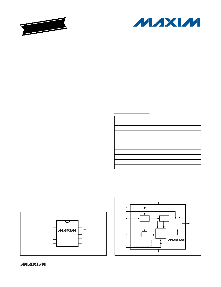
Functional Diagram
7
AIN
T/H
DOUT
6
1
OUTPUT
SHIFT
REGISTER
CONTROL
LOGIC
INT
CLOCK
12-BIT
SAR
8
2
3
5
REF
4
SHDN
2.5V REFERENCE
(MAX1240 ONLY)
GND
SCLK
CS
MAX1240
MAX1241
VDD
*Dice are specified at TA = +25°C, DC parameters only.
**Future product—contact factory for availability.
/V denotes an automotive qualified part.
+Denotes a lead(Pb)-free/RoHS-compliant package.
PART*
TEMP RANGE
PIN-
PACKAGE
INL
(LSB)
MAX1240ACPA+
0
°C to +70°C
8 PDIP
±1/2
MAX1240BCPA+
0
°C to +70°C
8 PDIP
±1
MAX1240CCPA+
0
°C to +70°C
8 PDIP
±1
MAX1240ACSA+
0
°C to +70°C
8 SO
±1/2
MAX1240BCSA+
0
°C to +70°C
8 SO
±1
MAX1240CCSA+
0
°C to +70°C
8 SO
±1
MAX1240CC/D
0
°C to +70°C
Dice*
±1
MAX1240AESA/V+**
-40
°C to +85°C 8 SO
±1/2
MAX1240BESA/V+
-40
°C to +85°C 8 SO
±1
For pricing, delivery, and ordering information, please contact Maxim Direct at 1-888-629-4642,
or visit Maxim’s website at www.maxim-ic.com.
发布紧急采购,3分钟左右您将得到回复。
相关PDF资料
MAX1245BCPP
IC ADC SRL 12BIT 2.375V 20-DIP
MAX1249AEPE+
IC ADC 10BIT SERIAL 16-DIP
MAX1279AETC+
IC ADC 12BIT 1.5MSPS 12-TQFN
MAX1285BESA+T
IC ADC 12BIT 300KSPS 8-SOIC
MAX1302BEUG+
IC ADC 16BIT SRL 115KSPS 24TSSOP
MAX1303BEUP+
IC ADC 16BIT MULT RANGE 20TSSOP
MAX1308ECM+T
IC ADC 12BIT 8CH 4MSPS 48LQFP
MAX1320ECM+T
IC ADC 14BIT 8CH 2MSPS 48LQFP
相关代理商/技术参数
MAX1240AESA
功能描述:模数转换器 - ADC RoHS:否 制造商:Texas Instruments 通道数量:2 结构:Sigma-Delta 转换速率:125 SPs to 8 KSPs 分辨率:24 bit 输入类型:Differential 信噪比:107 dB 接口类型:SPI 工作电源电压:1.7 V to 3.6 V, 2.7 V to 5.25 V 最大工作温度:+ 85 C 安装风格:SMD/SMT 封装 / 箱体:VQFN-32
MAX1240AESA/V+
功能描述:模数转换器 - ADC 12-Bit 73ksps 3.6V Precision ADC RoHS:否 制造商:Texas Instruments 通道数量:2 结构:Sigma-Delta 转换速率:125 SPs to 8 KSPs 分辨率:24 bit 输入类型:Differential 信噪比:107 dB 接口类型:SPI 工作电源电压:1.7 V to 3.6 V, 2.7 V to 5.25 V 最大工作温度:+ 85 C 安装风格:SMD/SMT 封装 / 箱体:VQFN-32
MAX1240AESA/V+T
功能描述:模数转换器 - ADC 12-Bit 73ksps 3.6V Precision ADC RoHS:否 制造商:Texas Instruments 通道数量:2 结构:Sigma-Delta 转换速率:125 SPs to 8 KSPs 分辨率:24 bit 输入类型:Differential 信噪比:107 dB 接口类型:SPI 工作电源电压:1.7 V to 3.6 V, 2.7 V to 5.25 V 最大工作温度:+ 85 C 安装风格:SMD/SMT 封装 / 箱体:VQFN-32
MAX1240AESA+
功能描述:模数转换器 - ADC 12-Bit 73ksps 3.6V Precision ADC RoHS:否 制造商:Texas Instruments 通道数量:2 结构:Sigma-Delta 转换速率:125 SPs to 8 KSPs 分辨率:24 bit 输入类型:Differential 信噪比:107 dB 接口类型:SPI 工作电源电压:1.7 V to 3.6 V, 2.7 V to 5.25 V 最大工作温度:+ 85 C 安装风格:SMD/SMT 封装 / 箱体:VQFN-32
MAX1240AESA+T
功能描述:模数转换器 - ADC 12-Bit 73ksps 3.6V Precision ADC RoHS:否 制造商:Texas Instruments 通道数量:2 结构:Sigma-Delta 转换速率:125 SPs to 8 KSPs 分辨率:24 bit 输入类型:Differential 信噪比:107 dB 接口类型:SPI 工作电源电压:1.7 V to 3.6 V, 2.7 V to 5.25 V 最大工作温度:+ 85 C 安装风格:SMD/SMT 封装 / 箱体:VQFN-32
MAX1240AESA-T
功能描述:模数转换器 - ADC RoHS:否 制造商:Texas Instruments 通道数量:2 结构:Sigma-Delta 转换速率:125 SPs to 8 KSPs 分辨率:24 bit 输入类型:Differential 信噪比:107 dB 接口类型:SPI 工作电源电压:1.7 V to 3.6 V, 2.7 V to 5.25 V 最大工作温度:+ 85 C 安装风格:SMD/SMT 封装 / 箱体:VQFN-32
MAX1240AMJA
功能描述:模数转换器 - ADC
RoHS:否 制造商:Texas Instruments 通道数量:2 结构:Sigma-Delta 转换速率:125 SPs to 8 KSPs 分辨率:24 bit 输入类型:Differential 信噪比:107 dB 接口类型:SPI 工作电源电压:1.7 V to 3.6 V, 2.7 V to 5.25 V 最大工作温度:+ 85 C 安装风格:SMD/SMT 封装 / 箱体:VQFN-32
MAX1240BCPA
功能描述:模数转换器 - ADC Integrated Circuits (ICs) RoHS:否 制造商:Texas Instruments 通道数量:2 结构:Sigma-Delta 转换速率:125 SPs to 8 KSPs 分辨率:24 bit 输入类型:Differential 信噪比:107 dB 接口类型:SPI 工作电源电压:1.7 V to 3.6 V, 2.7 V to 5.25 V 最大工作温度:+ 85 C 安装风格:SMD/SMT 封装 / 箱体:VQFN-32